
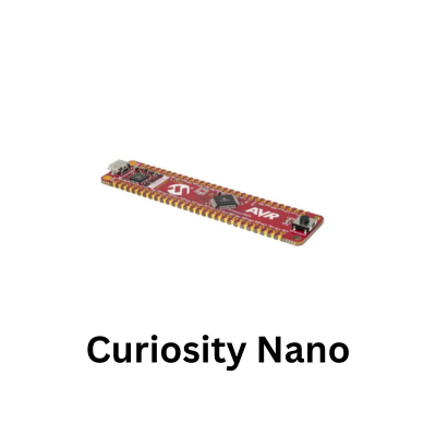
The ATmega4809 pinout is organised around six GPIO ports, PORTA through PORTF, with most pins capable of performing several functions depending on peripheral configuration and routing. A pin that operates as an ordinary digital input or output can often also serve a timer waveform output, ADC input, USART signal, SPI signal, TWI signal, event input or other peripheral function.
Understanding this multiplexing is essential when developing firmware on the ATmega4809 Curiosity Nano. A signal such as PA3 is not simply “digital pin 3.” It means pin 3 of PORTA, and its behaviour depends on the GPIO configuration, peripheral configuration and, for many peripherals, the selected PORTMUX route.
Three identities therefore need to remain separate when working with the Curiosity Nano: the ATmega4809 package pin, the logical port identifier such as PA3, and the physical connection exposed by the Curiosity Nano board. Firmware normally operates on the logical port identity, while wiring requires the Curiosity Nano board mapping. Never infer a physical header position from the port number alone.
The ATmega4809 also differs significantly from older AVR devices such as the ATmega328P. Code based on registers such as DDRB, PORTB, TCCR1A or the peripheral assumptions associated with classic Arduino-era AVR devices should not be transferred directly. The ATmega4809 uses the modern AVR PORT architecture, Virtual Ports, PORTMUX peripheral routing and newer timer, ADC and communication peripheral designs.
GPIO Ports and Pin Control
The general-purpose I/O system is divided into:
| Port | Logical pin range |
|---|---|
PORTA |
PA0–PA7 |
PORTB |
PB0–PB7 |
PORTC |
PC0–PC7 |
PORTD |
PD0–PD7 |
PORTE |
PE0–PE3 |
PORTF |
PF0–PF6 |
The existence of a logical port position does not by itself guarantee that the corresponding signal is available on every package or exposed on every Curiosity Nano header. Package bonding, dedicated functions and board routing must also be considered when selecting a physical connection.
Each port has registers for direction control, output control, input reading and per-pin configuration.
For PORTA, for example:
PORTA.DIR
PORTA.DIRSET
PORTA.DIRCLR
PORTA.DIRTGL

PORTA.OUT
PORTA.OUTSET
PORTA.OUTCLR
PORTA.OUTTGL

PORTA.IN
Individual pins also have control registers:
PORTA.PIN0CTRL
PORTA.PIN1CTRL
PORTA.PIN2CTRL
PORTA.PIN3CTRL
and so forth.
This architecture is worth understanding because it makes many GPIO operations both clearer and safer than traditional read-modify-write operations.
To configure PA3 as an output:
PORTA.DIRSET = PIN3_bm;
To configure it as an input:
PORTA.DIRCLR = PIN3_bm;
To drive the output high:
PORTA.OUTSET = PIN3_bm;
To drive it low:
PORTA.OUTCLR = PIN3_bm;
To toggle it:
PORTA.OUTTGL = PIN3_bm;
The set, clear and toggle registers operate on the bits written as ones. This avoids the conventional operation:
PORTA.OUT |= PIN3_bm;
which requires the processor to read the register, modify the value and write it back.
Atomic set and clear operations become particularly valuable when several execution contexts manipulate different bits of the same port.
Inputs are read from IN:
if (PORTA.IN & PIN4_bm)
{
    /* PA4 is high. */
}
The internal pull-up resistor for an input is configured through its PINnCTRL register:
PORTA.PIN4CTRL = PORT_PULLUPEN_bm;
For a pushbutton connected between PA4 and ground, the input therefore normally reads high while the switch is open and low when it is closed.
A complete GPIO initialization sequence might be:
#include <avr/io.h>

#define LED_bm     PIN3_bm
#define BUTTON_bm  PIN4_bm

static void gpio_init(void)
{
    /* Establish output state before enabling output driver. */
    PORTA.OUTCLR = LED_bm;
    PORTA.DIRSET = LED_bm;

    /* PA4 input with internal pull-up. */
    PORTA.DIRCLR = BUTTON_bm;
    PORTA.PIN4CTRL = PORT_PULLUPEN_bm;
}

int main(void)
{
    gpio_init();

    while (1)
    {
        if ((PORTA.IN & BUTTON_bm) == 0)
        {
            PORTA.OUTSET = LED_bm;
        }
        else
        {
            PORTA.OUTCLR = LED_bm;
        }
    }
}
This example deliberately refers to logical signals rather than claiming particular Curiosity Nano header positions. Before physically wiring PA3 or PA4, confirm where those signals are exposed on the specific Curiosity Nano board.
The PINnCTRL registers also control input sensing and pin inversion. Input sensing determines how a pin can generate interrupt requests and whether its digital input buffer is enabled in the selected configuration.
Virtual Ports and Peripheral Pin Routing
The ATmega4809 includes Virtual Ports, normally written as VPORTA, VPORTB and so forth. A VPORT provides a compact interface to the associated physical PORT.
For example:
VPORTA.DIR
VPORTA.OUT
VPORTA.IN
VPORTA.INTFLAGS
Virtual Ports are useful when code requires efficient single-cycle-style access to GPIO using the AVR I/O address space. The full PORT peripheral, however, provides the atomic SET, CLR and TGL registers and individual PINnCTRL configuration.
The two interfaces address the same underlying pins. They are not separate sets of GPIO.
Another important part of the ATmega4809 pin architecture is PORTMUX.
On many microcontrollers, a peripheral is permanently associated with one set of physical signals. The ATmega4809 instead allows several peripheral functions to be routed between predefined alternative pin groups.
This is particularly important for:
- USART
- SPI
- TWI
- TCA waveform outputs
- TCB waveform outputs
- CCL outputs
The exact alternatives are defined by the hardware. PORTMUX does not provide unrestricted routing from any peripheral to any arbitrary pin.
This distinction matters when laying out hardware. If an SPI peripheral needs to coexist with a USART and several PWM outputs, the firmware developer should determine the legal routes before committing the external wiring.
A common debugging mistake is configuring the peripheral correctly but connecting the external device to pins belonging to a different PORTMUX route.
In that situation, peripheral registers can appear completely correct while no useful waveform appears on the expected header.
When a USART, SPI, TWI or timer output appears inactive, checking PORTMUX should therefore be part of the diagnostic process.
Timers, PWM and Waveform Pins
The ATmega4809 timer architecture is substantially different from that of older AVR devices.
The principal timer resources include TCA and TCB peripherals, while additional timing capability is provided by the RTC and PIT.
TCA is a 16-bit Timer/Counter Type A. It is well suited to periodic timing and waveform generation and can provide multiple compare outputs.
A typical TCA configuration involves registers in the TCA0.SINGLE register group, including:
TCA0.SINGLE.CTRLA
TCA0.SINGLE.CTRLB
TCA0.SINGLE.CNT
TCA0.SINGLE.PER
TCA0.SINGLE.CMP0
TCA0.SINGLE.CMP1
TCA0.SINGLE.CMP2
TCA0.SINGLE.INTCTRL
TCA0.SINGLE.INTFLAGS
The period register determines the timer’s top value in appropriate operating modes, while compare registers determine compare events and waveform transitions.
PWM frequency depends on the peripheral clock, timer prescaler and period value.
Conceptually:
timer clock = peripheral clock / prescaler
and, for a single-slope PWM configuration:
PWM frequency = timer clock / (PER + 1)
The corresponding compare value determines duty cycle.
For approximately 50% duty cycle:
CMP ≈ (PER + 1) / 2
The exact output pin used by a TCA waveform depends on the available waveform channel and selected peripheral route. Configuring CMP0 correctly does not guarantee that a waveform will appear on whichever GPIO pin the application happens to select.
The GPIO/peripheral routing must also be correct.
TCB peripherals are Timer/Counter Type B modules. They can be used for periodic interrupts, time measurement, frequency measurement, capture functions and waveform-related applications.
TCA and TCB should not simply be viewed as “large timer” and “small timer.” Their operating modes differ, and one may be substantially better suited to a particular task.
The RTC occupies another timing domain and is particularly useful when long-duration timing or low-power operation is required. The Periodic Interrupt Timer associated with the RTC can generate regular periodic events without consuming a general-purpose timer.
When selecting pins for a design, timer output requirements should therefore be established before treating all unused GPIO pins as interchangeable.
ADC and Analog Functions
The ATmega4809 contains an ADC for converting supported analog input signals into digital values.
An analog input has two identities that must again be distinguished: the physical GPIO pin carrying the signal and the ADC multiplexer channel selected internally.
The ADC peripheral is controlled through ADC0 registers. Important configuration areas include control, reference, input selection, command, status and result handling.
A conversion requires several conditions to be correct:
- the physical analog signal must reach an ADC-capable pin;
- the input multiplexer must select the intended channel;
- an appropriate voltage reference must be configured;
- ADC timing must satisfy the peripheral requirements;
- the ADC must be enabled;
- a conversion must be started;
- firmware must wait for or respond to conversion completion before using the result.
The general conversion relationship is:
Vin ≈ ADC result × Vref / full-scale count
The exact interpretation depends on ADC operating mode and resolution.
A reading of zero therefore does not automatically mean the ADC is defective. It can indicate the wrong input channel, a signal actually at ground, an incorrect reference configuration, a conversion that never started or firmware reading the result at the wrong time.
Analog pin selection also has electrical consequences. High source impedance can affect the acquisition process because the ADC’s internal sampling circuitry must charge from the external signal source. Noise on the reference, power supply or input can produce conversion variation.
Software averaging can reduce random variation, but it cannot correct an inaccurate reference voltage or systematic analog error.
For applications that only need to determine whether one voltage is above or below another, the ATmega4809 Analog Comparator may be preferable to repeatedly sampling the ADC. The comparator can produce a hardware decision without requiring the CPU to process a stream of conversion results.
USART, SPI and TWI Pins
Communication peripherals are another area where pin multiplexing becomes important.
The ATmega4809 provides USART hardware for asynchronous and synchronous serial communication. A conventional asynchronous interface requires at least transmit and receive signals.
Firmware must configure both the USART and the appropriate routing.
The USART configuration establishes characteristics including baud rate, data length, parity and stop bits. The selected route determines where the peripheral’s signals appear physically.
Baud-rate configuration is dependent on the peripheral clock. A baud register value copied from a project running at a different clock frequency can therefore produce corrupted communication even though the TX and RX wiring is correct.
When debugging USART communication, first measure or verify the actual clock assumption, then confirm the peripheral route and physical pins, and only then investigate terminal settings or buffering.
SPI has similar routing considerations.
An SPI master normally requires:
MOSI
MISO
SCK
SS/CS
The ATmega4809 SPI peripheral generates the serial clock in master mode and shifts data synchronously.
External devices also require a particular SPI mode. Clock polarity and clock phase determine when data changes and when it is sampled.
Correct pin wiring with the wrong mode commonly produces data that looks random or consistently incorrect.
Multiple SPI peripherals can normally share MOSI, MISO and SCK while using separate chip-select signals. Chip select is often managed as an ordinary GPIO output.
For example:
PORTA.OUTSET = PIN7_bm;
PORTA.DIRSET = PIN7_bm;
could establish an initially inactive active-low chip-select on a deliberately selected GPIO, assuming PA7 is actually available and wired for that purpose in the application.
A transaction would assert the signal:
PORTA.OUTCLR = PIN7_bm;
perform the SPI transfer, and then release it:
PORTA.OUTSET = PIN7_bm;
TWI is the ATmega4809 peripheral used for I2C-compatible communication. Its external signals are SDA and SCL.
Unlike ordinary push-pull digital interfaces, I2C uses open-drain/open-collector-style signalling. SDA and SCL therefore require pull-up resistors to an appropriate logic supply.
A missing pull-up can make an otherwise correct TWI program appear completely non-functional.
The physical route again matters. Configuring TWI does not cause SDA and SCL to appear on arbitrary GPIO pins.
When an I2C peripheral does not acknowledge, examine the actual SDA and SCL lines. Both should normally be high while the bus is idle. If either remains low before a transaction begins, there is an electrical problem, a device holding the bus, incorrect wiring or a previous transaction that left the bus in an abnormal state.
A logic analyser can then confirm START conditions, addresses, ACK/NACK responses and STOP conditions.
Event System, CCL and Other Pin-Related Resources
The ATmega4809 Event System is primarily an internal routing mechanism rather than an external pin interface, but it has significant implications for how pins and peripherals can interact.
An event generator can produce an internal event that is carried over an event channel to an event user.
Instead of processing an external transition in software, firmware can configure hardware so that the transition causes another peripheral action directly.
Conceptually:
Pin/peripheral event
        |
        v
Event generator
        |
        v
Event channel
        |
        v
Peripheral event user
No interrupt handler is inherently required for that path.
This is valuable for deterministic timing. An interrupt-based solution includes interrupt recognition latency, context handling and ISR execution. An Event System connection can transfer the event directly in hardware.
The Configurable Custom Logic peripheral extends this idea by implementing small logic functions within the MCU.
CCL inputs can originate from supported internal or external sources. Lookup tables implement the required logical relationship, and outputs can feed other internal hardware or supported external output routes.
For example, hardware logic may combine an enable condition and a timer-related signal without requiring the CPU to evaluate both inputs continuously.
CCL should not be used merely because it exists. Straightforward application logic often remains clearer in C. It becomes particularly useful when latency, deterministic behaviour, low-power operation or CPU-independent signal processing matters.
Other pin-related functions include the external clock system, UPDI programming/debugging interface and reset-related behaviour. These signals should not be treated casually as spare GPIO simply because a package position appears physically accessible.
UPDI is especially important on the Curiosity Nano because it is used by the onboard debugger to program and debug the ATmega4809. A design that interferes with the programming/debug path can make firmware development considerably more difficult.
Electrical Considerations When Using the Pinout
A pinout identifies connectivity and alternate functions; it does not define a safe load by itself.
An ATmega4809 GPIO output should be treated as a logic output with limited current capability. It is suitable for driving logic inputs and low-current indicator circuits when the electrical limits are respected.
An LED requires a series resistor.
A motor does not belong directly on a GPIO.
Neither does a relay coil, solenoid or other substantial inductive load.
Such loads require an appropriate transistor, MOSFET or driver IC. Inductive loads normally require suppression such as a flyback diode, and the external load supply must be selected for the load rather than expecting the Curiosity Nano GPIO to supply it.
A common ground is normally required when the ATmega4809 communicates with externally powered circuitry through ordinary ground-referenced digital signals.
Voltage compatibility must also be checked. A peripheral powered at a higher logic voltage must not simply be connected to an ATmega4809 input unless the resulting signal remains within the permitted electrical limits. A level shifter or appropriate interface may be necessary.
I2C deserves particular attention because its pull-up resistors establish the bus high voltage. Pulling SDA and SCL to a voltage unsuitable for the ATmega4809 can expose the MCU pins to an invalid level even though the I2C device itself operates correctly.
Analog signals require the same discipline. An ADC-capable pin does not become tolerant of arbitrary analog voltage simply because the ADC is selected. The applied voltage must remain within the permitted electrical range.
Diagnosing Pin and Peripheral Problems
Pin-related failures are easiest to solve by separating firmware configuration from physical routing.
Suppose a GPIO output does not change voltage.
First inspect its DIR bit. If the direction is not output, the problem is firmware initialization.
Next inspect OUT. If the output latch changes but the pin does not, the problem has moved downstream. Check whether the correct physical signal is being measured, whether a peripheral function has been routed to that pin, and whether external circuitry is forcing the voltage.
If the output changes correctly at the microcontroller connection but not at an attached peripheral, investigate the board wiring.
An input permanently reading high should be measured electrically. If the pin physically remains high when the external circuit should pull it low, firmware is unlikely to be the immediate cause. Check wiring, common ground, switch connections and external pull resistors.
If the physical pin goes low but PORTx.IN reports high, verify the selected port and bit.
A PWM peripheral that counts correctly but produces no external waveform strongly suggests a routing problem. Inspect TCA or TCB status and count registers. If the counter advances and compare events occur, check the waveform enable configuration and PORTMUX route before rewriting the timing calculations.
For a silent USART, determine whether TX physically toggles. If it does not, check peripheral enable and routing. If it does toggle but the receiving terminal displays corrupt characters, measure the bit timing and compare it with the intended baud rate.
For SPI, inspect SCK first. No clock normally means the master has not started a transaction, the peripheral is not enabled, or the wrong pin route is being observed. A valid clock with invalid returned data shifts attention toward chip select, SPI mode, wiring and the external device’s protocol.
For TWI, inspect the idle bus before examining firmware transactions. SDA and SCL should normally both be high. A permanently low line is an electrical or bus-state problem that should be resolved before interpreting address ACK behaviour.
Register inspection is particularly effective on the ATmega4809 because it can establish whether the hardware configuration agrees with the source code’s intention.
The Curiosity Nano onboard debugger can inspect PORTx.DIR, PORTx.OUT, peripheral control registers, status registers and timer counters while developing the application.
For static GPIO states, a multimeter is usually sufficient. For PWM, serial communication, SPI, TWI and short event pulses, a logic analyser or oscilloscope provides substantially more information.
A useful debugging technique is also to reserve one spare GPIO as a firmware marker:
PORTA.OUTSET = PIN5_bm;

/* Operation under test. */

PORTA.OUTCLR = PIN5_bm;
The resulting pulse can show exactly when firmware enters and leaves an operation without inserting serial output that changes execution timing.
Using the Pinout When Designing Real Hardware
The correct time to plan peripheral pin allocation is before hardware wiring becomes fixed.
Start with functions that have the fewest routing choices or the strongest electrical constraints. Programming/debug signals and power connections are effectively fixed. Analog signals need suitable ADC-capable inputs. Communication peripherals must use supported peripheral routes. Hardware PWM outputs must correspond to valid timer waveform routes.
Only after those constraints are established should remaining pins be allocated to generic buttons, LEDs, chip-select signals and other ordinary GPIO functions.
This becomes particularly important when several peripherals are used simultaneously. A design may require an SPI sensor, I2C environmental sensors, USART debugging, several PWM outputs, analog measurements and external interrupts. There may be enough GPIO pins numerically, yet an inconvenient selection of peripheral routes can still create conflicts.
PORTMUX can solve many of these conflicts, but only within the routes implemented by the ATmega4809.
For each signal in a real project, it is useful to record at least:
| Design property | Example information |
|---|---|
| Application function | Sensor interrupt |
| MCU signal | PA4 |
| GPIO port | PORTA |
| Direction | Input |
| Electrical configuration | Internal pull-up |
| Peripheral function | GPIO interrupt |
| Active state | Low |
| External voltage | MCU-compatible logic level |
For communication or timer pins, add the peripheral instance and selected PORTMUX route.
This simple discipline prevents a frequent embedded development problem: firmware referring to one naming convention while the schematic, board header and peripheral route refer to another.
Pin allocation should also leave room for debugging where practical. A spare GPIO that can be connected to a logic analyser is often more valuable during development than using every available signal immediately.
The ATmega4809 pinout is therefore best treated as part of the microcontroller’s peripheral architecture rather than as a list of digital pin numbers. PORTA through PORTF, PINnCTRL, Virtual Ports and PORTMUX together determine how external signals interact with GPIO, timers, communication peripherals, analog functions, the Event System and CCL.
Once you understand those relationships, pin selection becomes a design task, not a trial and error task: determine the peripheral requirement, find out the legal routes to it, make sure that the required MCU signal is exposed by the Curiosity Nano, verify its electrical compatibility, configure the relevant peripheral and PORT registers, and finally measure the physical signal to confirm that the hardware performs as expected.