
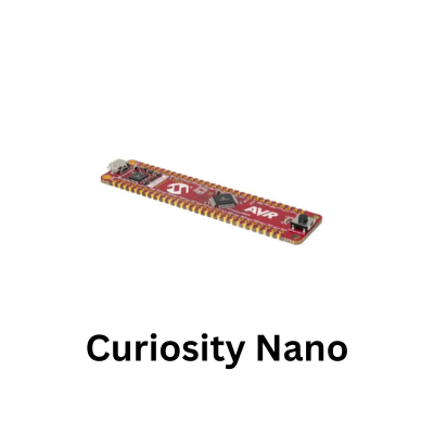
The ATmega4809 Curiosity Nano is a compact development board built around Microchip’s ATmega4809, a modern member of the AVR family. Although the processor executes the familiar AVR instruction set, its peripheral architecture differs substantially from older devices such as the ATmega328P. GPIO configuration, timers, clock control, interrupts, ADC operation and peripheral routing all use the newer AVR architecture. Code written directly against registers such as DDRB, PORTB and TCCR1A on an older AVR therefore cannot simply be transferred to the ATmega4809.
The Curiosity Nano board provides the ATmega4809, USB-powered operation, an onboard debugger/programmer and access to the microcontroller signals through the board headers. This makes it possible to move beyond simple framework-level programming and work directly with the microcontroller hardware without requiring a separate programming tool.
A useful first firmware project is deliberately simple: configure a GPIO output, toggle it at a controlled rate, compile and program the device, and then inspect the resulting hardware state. That exercise establishes the entire development path while introducing one of the most important architectural differences between the ATmega4809 and older AVR devices: its PORT peripheral and atomic set, clear and toggle registers.
Once that basic path is working, the same development environment can be used for the ATmega4809’s timers, ADC, USART, SPI, TWI, Event System, Configurable Custom Logic and other peripherals.
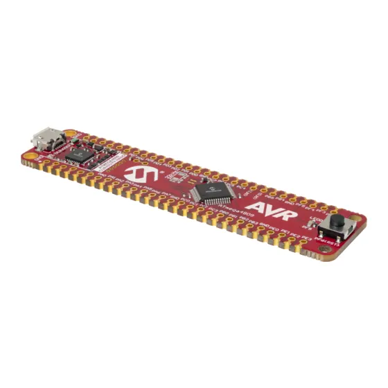
atmega4809-curiosity-nano-motherboard
Understanding the Curiosity Nano Hardware
The Curiosity Nano is more than an ATmega4809 mounted on a breakout board. It combines the target microcontroller with an onboard debugger that provides programming and debugging through the USB connection. This arrangement eliminates the separate ISP programmer normally associated with traditional AVR development.
The debugger communicates with the ATmega4809 using its UPDI programming and debugging interface. UPDI is the modern AVR programming interface used by the ATmega4809 and many related devices. From the firmware developer’s perspective, the important consequence is that the board can normally be connected directly to a development computer over USB and programmed without adding a separate programmer.
Most application signals are exposed through the Curiosity Nano edge connections. When the board is installed in a Curiosity Nano Explorer or connected to a breadboard, those signals can be connected to switches, LEDs, sensors and communication devices.
Three different forms of pin identification must not be confused.
A physical Curiosity Nano header position identifies where a signal appears on the development board. The microcontroller package pin identifies a physical lead on the ATmega4809 itself. A name such as PA3 or PB2 identifies the logical GPIO signal within the AVR PORT peripheral.
Firmware generally works with the logical GPIO identity. For example, PA3 means bit 3 of PORTA. The corresponding firmware operations therefore use registers such as PORTA.DIRSET, PORTA.OUTSET and PORTA.PIN3CTRL.
The physical Curiosity Nano connection corresponding to that signal must be confirmed from the board pinout for the particular board revision before wiring external hardware. Do not infer a header position merely from the PA3 designation.
Power is equally important. External circuits need a common ground with the Curiosity Nano, and signals applied to the ATmega4809 must remain within the permitted voltage range for the selected operating supply. GPIO pins are logic signals, not general-purpose power outputs. Motors, relays, solenoids, high-current lamps and similar loads require an appropriate transistor, MOSFET or driver stage rather than being connected directly to a GPIO pin.
An external LED also requires a series current-limiting resistor. Values such as 330 Ω to 1 kΩ are commonly suitable for a simple indicator circuit, depending on LED forward voltage and required brightness. The resistor limits the current flowing through both the LED and the microcontroller output driver.
For initial experiments, the Curiosity Nano Explorer is useful but not mandatory. A breadboard, jumper wires, an LED and resistor are sufficient for basic GPIO testing.
Setting Up a Register-Level AVR Project
A straightforward ATmega4809 development environment consists of MPLAB X IDE with an AVR-capable XC8 installation. AVR-GCC-based environments can also be used. The examples here use standard AVR C constructs and the device definitions supplied by the AVR toolchain.
The central include is:
#include <avr/io.h>
This provides the ATmega4809 register and bit definitions selected by the project device configuration.
For interrupt-driven programs, the interrupt definitions are also required:
#include <avr/interrupt.h>
A delay-based test may use:
#include <util/delay.h>
when compiling with AVR-GCC-compatible headers and when F_CPU correctly describes the CPU clock used by the delay implementation.
The target device must explicitly be configured as the ATmega4809. Selecting the wrong AVR can produce incorrect register definitions, incorrect startup configuration or a program that cannot be programmed into the target.
A minimal application has the familiar form:
#include <avr/io.h>

int main(void)
{
    while (1)
    {
    }
}
There is no operating system and normally no automatic return from main(). After reset, the startup code establishes the C runtime environment and eventually calls main(). Firmware then remains inside the main loop while peripherals and interrupts perform the required work.
One of the first useful checks is to make an external GPIO change state. Using an external LED avoids depending on assumptions about the polarity or routing of a board-mounted indicator.
Suppose an LED is intentionally connected to PA3 through an appropriate series resistor. That choice is an example connection rather than an assertion that PA3 corresponds to a particular onboard LED.
The pin is configured as an output with:
PORTA.DIRSET = PIN3_bm;
PIN3_bm is a mask with bit 3 set. Writing that mask to DIRSET sets the corresponding bit in the port direction register.
The output can then be controlled using:
PORTA.OUTSET = PIN3_bm;
PORTA.OUTCLR = PIN3_bm;
PORTA.OUTTGL = PIN3_bm;
These operations demonstrate an important feature of the newer AVR PORT peripheral.
Older AVR programs commonly manipulate a port using read-modify-write operations:
PORTB |= (1 << 3);
The ATmega4809 provides dedicated set, clear and toggle registers. Writing a one to a bit in OUTSET sets the corresponding output latch bit. Writing a one to OUTCLR clears it, and writing a one to OUTTGL toggles it.
The same principle applies to direction registers through DIRSET, DIRCLR and DIRTGL.
This is particularly useful in interrupt-driven firmware because an atomic set or clear operation does not require software to read the complete register, modify one bit and write the complete value back. It reduces the possibility of unrelated port bits being unintentionally affected.
A simple GPIO test program is:
#ifndef F_CPU
#define F_CPU 3333333UL
#endif

#include <avr/io.h>
#include <util/delay.h>

#define TEST_LED_bm PIN3_bm

static void gpio_init(void)
{
    PORTA.OUTCLR = TEST_LED_bm;
    PORTA.DIRSET = TEST_LED_bm;
}

int main(void)
{
    gpio_init();

    while (1)
    {
        PORTA.OUTTGL = TEST_LED_bm;
        _delay_ms(500);
    }
}
This assumes that the project’s actual CPU clock matches the F_CPU value used for the delay calculation. That assumption must be verified for the project configuration rather than copied blindly into other applications.
The order inside gpio_init() is intentional. The desired initial output latch state is established before the pin is enabled as an output. This is useful in real hardware because it prevents a load from momentarily seeing an unintended output level during initialization.
If the LED changes state every 500 ms, one complete on/off cycle takes approximately one second.
The important word is approximately. _delay_ms() depends on the configured CPU frequency, compiler implementation and oscillator accuracy. It is useful for an initial hardware test but is not a good foundation for applications requiring accurate scheduling or simultaneous execution of other tasks.
GPIO Inputs and the Modern PORT Peripheral
A second useful experiment is reading a pushbutton. An input should never be assumed to have a defined logic state unless the external circuit or an internal pull resistor provides one.
A floating digital input can respond to electrical noise, leakage current, nearby wiring and even a person’s hand approaching the circuit. A button connected between an input and ground therefore normally uses a pull-up resistor so that the input is high while the button is released and low while it is pressed.
On the ATmega4809, individual pin behaviour is configured using PINnCTRL registers.
For example:
PORTA.PIN4CTRL = PORT_PULLUPEN_bm;
enables the internal pull-up for PA4.
The pin direction can explicitly be made input using:
PORTA.DIRCLR = PIN4_bm;
The state is then read through the port input register:
if ((PORTA.IN & PIN4_bm) == 0)
{
    /* Input is low. */
}
For a button wired between PA4 and ground, low means pressed.
A complete example controlling the LED from the button is:
#include <avr/io.h>

#define LED_bm     PIN3_bm
#define BUTTON_bm  PIN4_bm

static void gpio_init(void)
{
    PORTA.OUTCLR = LED_bm;
    PORTA.DIRSET = LED_bm;

    PORTA.DIRCLR = BUTTON_bm;
    PORTA.PIN4CTRL = PORT_PULLUPEN_bm;
}

int main(void)
{
    gpio_init();

    while (1)
    {
        if ((PORTA.IN & BUTTON_bm) == 0)
        {
            PORTA.OUTSET = LED_bm;
        }
        else
        {
            PORTA.OUTCLR = LED_bm;
        }
    }
}
This program is intentionally polling the button. The CPU repeatedly reads PORTA.IN and updates the output.
For a first experiment, polling is useful because there are few moving parts. If the LED behaves incorrectly, the developer only needs to investigate the wiring, port configuration and input state rather than an interrupt controller as well.
It also demonstrates active-low logic. With the pull-up enabled, the released state is logic high. Closing the button connects the input to ground and produces logic low.
Real mechanical switches bounce. Their contacts can open and close several times during the transition from one physical state to another. That does not matter much when the LED simply follows the button, but it becomes important if every transition increments a counter or changes an application state.
Debouncing can be implemented in software using timer-based state validation, or in hardware where the application requires it. A long blocking delay after detecting a button press is easy to write but becomes undesirable as firmware grows because the processor cannot perform other scheduled work during that delay.
The PINnCTRL registers provide more than pull-up configuration. They also control input sensing behaviour and, where appropriate, inversion. This is another difference from traditional AVR designs in which interrupt configuration may be concentrated in separate external-interrupt registers.
Moving from Delays to Hardware Timers
A delay loop demonstrates that the processor is executing instructions, but it also monopolizes the CPU. The ATmega4809 provides several timer/counter peripherals designed to generate timing events independently of application code.
The most important timer families are TCA and TCB. TCA is a flexible 16-bit timer/counter with waveform-generation capabilities and multiple compare channels. TCB is a smaller timer/counter architecture suited to periodic timing, capture and other specialized tasks.
For a periodic firmware heartbeat, timer interrupts are preferable to a chain of software delays. The processor can perform useful work between timer events.
The fundamental timer relationship is:
timer frequency = peripheral clock / prescaler
If a timer counts from zero through a defined terminal count, the interrupt period depends on the number of timer ticks in that interval.
For a timer using a count value N:
period = timer ticks × timer tick period
or equivalently:
required ticks = desired period × timer frequency
These calculations should always precede the register values placed in firmware. Copying timer constants from another project is dangerous because a different CPU or peripheral clock changes the resulting time.
The ATmega4809 clock configuration therefore matters throughout the application. A USART baud-rate setting, PWM period, timer interval and software delay can all become incorrect when code assumes a clock frequency different from the hardware’s actual frequency.
This is one reason a new ATmega4809 project should establish its clock assumptions explicitly.
For production firmware, clock configuration should be treated as part of the hardware abstraction for the application rather than an incidental startup detail. If the CPU clock changes to reduce power consumption, every peripheral whose timing is derived from that clock must either be reconfigured or designed so that the change does not invalidate its operation.
The ATmega4809 Peripheral Architecture
Once basic GPIO operation has been verified, it is useful to understand how the rest of the device fits together. The ATmega4809 contains considerably more peripheral hardware than is required for a blinking LED, and many of its features are intended to reduce CPU involvement.
TCA provides general timing and PWM generation. TCB timers can be used for periodic timing, event counting, frequency measurement and related functions. The RTC provides timing from a clock domain suitable for longer-period operation, while the Periodic Interrupt Timer can generate regular events without consuming a general-purpose timer.
The ADC converts analog input voltages into digital results. An Analog Comparator can make a hardware decision about two analog levels without repeatedly starting ADC conversions.
USART peripherals provide asynchronous serial communication. SPI provides synchronous full-duplex communication commonly used with sensors, displays, memories and converters. The TWI peripheral implements the hardware required for I2C-compatible communication.
Two particularly useful modern AVR features are the Event System and Configurable Custom Logic.
The Event System allows one peripheral to trigger another through hardware. Instead of an interrupt occurring, the CPU entering an ISR, software manipulating a register and then returning, an event can travel directly between hardware peripherals.
For example, a timer event may trigger another peripheral without software executing at the instant of the event. This reduces interrupt latency and CPU loading and can make timing much more deterministic.
CCL provides small programmable logic functions inside the microcontroller. Logic inputs can originate from pins or internal signals, pass through configurable lookup-table logic and produce internal or external outputs.
These capabilities change the way an ATmega4809 system can be designed. A traditional AVR solution may involve several interrupts and software state transitions, while an ATmega4809 implementation may move part of the signal processing into the Event System and CCL.
This is not automatically the correct solution for every application. A simple low-frequency user-interface function may be clearer in ordinary C. Hardware event routing becomes particularly valuable when deterministic timing, low CPU overhead or operation during sleep is important.
Building and Debugging the First Firmware
After the project has been configured for the ATmega4809, the source should compile without warnings caused by undeclared registers, incorrect bit masks or missing device definitions.
Programming the Curiosity Nano should then cause the debugger to erase and program the target Flash before allowing the processor to run.
If the first GPIO test does not work, changing the program repeatedly without measurements is inefficient. The objective is to establish where the expected state stops matching reality.
Start with the output direction.
If PA3 is supposed to be an output, inspect PORTA.DIR in the debugger. Bit 3 should indicate output configuration after gpio_init() has executed.
Next inspect the output latch. PORTA.OUT should change when the firmware writes to PORTA.OUTTGL.
Those two observations divide the problem into useful categories.
If PORTA.DIR is wrong, initialization has not executed correctly, the program may not be reaching the expected code, or the wrong port/pin is being inspected.
If PORTA.DIR is correct but PORTA.OUT never changes, the main loop or toggle operation is not executing as expected.
If both registers change correctly but the external pin does not change voltage, the problem is likely to involve pin identification, physical wiring, an external load or another peripheral controlling the pin.
A multimeter can verify a static output without requiring an oscilloscope. Temporarily replace the toggle loop with a permanently high output:
PORTA.OUTSET = PIN3_bm;
The pin should then sit near the logic-high supply level when unloaded or lightly loaded.
Similarly:
PORTA.OUTCLR = PIN3_bm;
should produce a voltage near ground.
A logic analyser or oscilloscope becomes more useful when examining timing. If the output is toggled every 500 ms, either instrument should show transitions approximately 500 ms apart.
The onboard debugger also permits breakpoints and single stepping. A breakpoint after initialization can confirm that startup completed. Register inspection can then establish whether the peripheral state matches the intended configuration.
There is one important caution with debugging timing-sensitive firmware: stopping the CPU changes the behaviour of the system. Peripherals may not all respond to debugging halts in the same way, and an external device continues operating while firmware is stopped. A breakpoint is therefore excellent for inspecting initialization but may be inappropriate for diagnosing a communication protocol whose timing must remain continuous.
For those cases, a spare GPIO used as a timing marker is extremely useful:
PORTA.OUTSET = PIN5_bm;

/* Code being measured. */

PORTA.OUTCLR = PIN5_bm;
An oscilloscope or logic analyser can measure the resulting pulse width without disturbing execution.
Common Failure Modes and Diagnostic Reasoning
An LED that never illuminates has several possible causes, and each can be tested independently.
First establish whether the expected physical pin is being used. A logical definition such as PA3 does not identify a Curiosity Nano header position by itself. Verify the board signal mapping and then use continuity testing if necessary to confirm the external circuit reaches the intended connection.
Next inspect PORTA.DIR. If bit 3 is not configured for output, the external pin is not being actively driven by the GPIO output stage. Check whether gpio_init() executes and whether the correct mask is being written.
If the direction is correct, inspect PORTA.OUT. Force the output high and low instead of toggling it. Measure the pin voltage with a multimeter. If the register changes but the physical voltage does not, investigate physical pin selection, external loading and whether another peripheral has ownership of the output path.
If the voltage changes correctly but the LED remains dark, inspect the LED orientation, series resistor and wiring.
A button that always reads high is another common problem. With an internal pull-up enabled, a disconnected input legitimately reads high. If pressing the button does not pull the pin low, use a multimeter to measure the actual voltage on the GPIO connection while the button is pressed.
If the voltage remains high, the problem is electrical: the button is not connecting the signal to ground, the wrong switch contacts have been used, the wrong board pin is connected, or ground is missing.
If the voltage falls to ground but PORTA.IN remains high, verify that the software is reading the same port and pin being measured physically.
An input that changes randomly usually indicates a floating signal. Verify that the pull-up has actually been enabled in the correct PINnCTRL register and that no external circuit is overpowering it.
A program that runs but has incorrect delays frequently indicates a clock assumption error. The value assigned to F_CPU does not configure the hardware clock. It tells software such as delay routines what frequency to assume. Defining F_CPU as 20 MHz while the processor actually runs at another frequency does not make the processor run at 20 MHz; it merely causes calculations based on that definition to be wrong.
The same principle later applies to timer calculations and serial baud rates.
Garbled USART output is therefore often a clock problem rather than a serial-terminal problem. A correct frame format with an incorrect baud clock still produces unreadable characters.
A peripheral that appears completely inactive should be debugged in layers. Confirm the system clock. Confirm that the peripheral has been initialized. Confirm its pin routing. Inspect the peripheral registers. Check status and interrupt flags. Finally measure the actual external signal.
This approach is much faster than making several unrelated code changes simultaneously.
Electrical and Firmware Practices Worth Establishing Early
The first experiments on a development board often become templates for later projects, so good habits are useful even when they seem unnecessary for a single LED.
Set an output’s initial latch state before enabling its output driver. This prevents unwanted startup transitions.
Use DIRSET, DIRCLR, OUTSET, OUTCLR and OUTTGL when manipulating individual GPIO bits. These registers express the intended operation clearly and avoid unnecessary software read-modify-write sequences.
Do not repeatedly write complete peripheral registers when only one bit needs to change unless replacing the complete register value is intentional.
Keep hardware configuration in initialization functions rather than scattering register writes throughout application logic. A larger application might contain functions such as:
static void clock_init(void);
static void gpio_init(void);
static void timer_init(void);
static void adc_init(void);
static void usart_init(void);
This makes the initialization sequence visible and simplifies debugger inspection.
For interrupt-driven code, variables shared between an ISR and normal execution generally require volatile when their value can change asynchronously from the compiler’s perspective.
For example:
static volatile uint8_t timer_event;
An ISR might set the flag:
timer_event = 1;
and the main loop could process it:
if (timer_event)
{
    timer_event = 0;
    process_periodic_task();
}
The ISR should normally do only the work required at interrupt time. Long delays, formatted serial output and large processing routines inside an ISR increase interrupt latency and make system timing harder to reason about.
volatile does not itself make multi-byte operations atomic. If the main program and an ISR share a value wider than the processor can safely access as a single indivisible operation, synchronization may still be required.
Similar discipline applies to external hardware. GPIO outputs should drive logic inputs, LEDs at suitable current, or the control input of an external driver. They should not directly power loads simply because a load happens to operate from the same nominal voltage.
Inductive loads require particular care. A relay coil, solenoid or motor should be controlled through a suitable driver, with protection such as a flyback diode where required. External supplies must normally share a reference ground with the Curiosity Nano when ordinary single-ended logic signals pass between them.
Communication buses add their own electrical requirements. I2C/TWI uses open-drain signalling and therefore requires suitable pull-up resistors on SDA and SCL. SPI normally uses actively driven logic signals but requires compatible voltage levels and correct chip-select handling. None of these requirements is fixed by software.
Where to Go After GPIO
Once the development environment, debugger and GPIO operations are verified, it is better to progress through peripherals in a deliberate order rather than immediately combining several subsystems.
Timer operation is a useful next step because it establishes clock calculations, peripheral initialization, interrupt flags and ISRs. Replace the blocking LED delay with a timer-generated periodic event and verify the period with a logic analyser or oscilloscope.
PWM then extends the timer work. Instead of merely producing periodic interrupts, configure a timer waveform output and derive both the period and compare values from the required frequency and duty cycle. This demonstrates the relationship between clock frequency, prescaling, counter range and PWM resolution.
ADC operation introduces analog references, input channels, conversion timing and conversion of raw counts into physical voltage. ADC debugging should include measurement of the actual input voltage with a multimeter rather than assuming the external signal is correct.
USART is an effective introduction to communications because a terminal can provide immediate diagnostic output. The baud-rate configuration must be derived from the actual peripheral clock. Once blocking transmit and receive operation is understood, buffering and interrupts can be added.
SPI and TWI should then be approached as electrical buses as well as software peripherals. For SPI, verify mode, clock frequency, chip select and voltage compatibility against the attached device. For TWI, verify SDA and SCL pull-ups, address behaviour, bus voltage and ACK/NACK state before assuming a software transaction is wrong.
The Event System and CCL become most useful after conventional timers and interrupts are understood. Their advantage is easier to appreciate when there is already a working software implementation to compare against. Moving a repetitive or timing-critical relationship from an ISR into hardware can reduce CPU intervention and improve timing determinism.
Low-power operation should similarly be measured rather than assumed. Putting the CPU into a sleep mode does not guarantee that an entire board will consume the microcontroller’s datasheet sleep current. The debugger, regulator, LEDs, pull resistors and external circuitry can dominate board-level current consumption. Current measurements therefore need to specify what hardware is connected and which portions of the board remain powered.
The Curiosity Nano is particularly useful through these stages because the same board can support basic register-level experiments and substantially more advanced firmware. There is no need to abandon the development platform when moving from GPIO into timers, ADC, communication buses, interrupts or hardware event routing.
The important transition is in the firmware architecture: begin with simple polling when it makes behaviour easy to observe, introduce interrupts when asynchronous response is useful, and use autonomous peripherals or the Event System when hardware can perform the operation more predictably without constant CPU involvement.
Before integrating any experiment into a larger application, verify the assumptions on which it depends: the actual CPU and peripheral clocks, physical pin mapping, pin direction, electrical voltage levels, peripheral routing, interrupt behaviour and external signal timing. Those checks turn a demonstration that appears to work into firmware whose behaviour can be explained and reproduced on real hardware.